

MiDFUN Product Module / AOI
Automated optical inspection for wafer, packaging, and PCB workflows
AOI supports image-based defect and dimensional inspection for semiconductor, packaging, and PCB use cases where speed and consistency are critical.
Best Fit
- Wafer probe-mark and defect inspection
- Packaging and bumping dimensional checks
- PCB automated inspection and drill-data comparison
Key Capabilities
- Automated image inspection and defect counting
- Dimensional measurement and reporting
- Inspection data for quality and MES integration
QRP Data Flow
AOI converts optical inspection results into quality records that can support process review, SPC, and customer-quality reporting.

Probe Mark Inspection:
This system provides professional wafer probe-mark defect measurement and statistical analysis. Selected by leading wafer fabs and IC test/material suppliers such as TSMC, ASE Group, ASE Test, and Taiwan Union Technology (TUC), it supports probe-mark area measurement and analysis, wafer defect image analysis, high-speed defect counting, probe-mark defect area-ratio calculation, and relative distance calculation, and can rapidly generate defect inspection statistical reports.

Bumping Process A.O.I. Rapid Automated Dimensional Inspection
On the production floor of the packaging and test industry, the metallographic microscope performs automated inspection of circle diameters and various dimensions without manual edge-finding or point-picking, and can save image files. Measurement results are provided directly for integration with in-plant quality management or the MES system, achieving the goal of automated measurement quality.


PCB – Automated Inspection for the Printed Circuit Board Industry
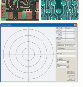
- Load an NC drilling file to automatically generate a macro, enabling immediate automated measurement. Results can be compared against the drilling-file standard, and nonconforming items automatically turn red as a warning, making product quality clear at a glance.
- Drilling-file measurement results can generate a drill-position scatter plot via the MiDFUN SPC function, tallying the count within each offset interval to provide a basis for parameter adjustment on the NC drilling machine.
- Panelized boards, multilayer boards, and symmetrical boards are measured automatically in a single pass.
- Automatic interval circle-finding: the system provides an automatic nearest-circle finding function on the image view, making measurement more efficient.