


最後更新:2026.06.22
About Xintec Inc.
Xintec Inc. was founded in 1998 and is located in the Chungli Industrial Zone in Taiwan. It is the first company to commercialize three-dimensional stacked wafer-level chip-scale packaging (3D WLCSP) technology. Xintec engages in the wafer-level packaging production of CMOS image sensor devices and delivers an optimal production cycle along with highly competitive production costs. Thanks to its strong product integration capabilities, three-dimensional stacked wafer-level packaging technology can be applied across a wide range of market segments such as consumer electronics, communications, computing, industrial, and automotive. Product applications include image sensors, optical sensors, power management integrated circuits, power discrete devices, analog integrated circuits, mixed-signal integrated circuits, MEMS sensors, and integrated passive devices.
Xintec engages in innovative three-dimensional stacked wafer-level packaging manufacturing services, with “integrity, innovation, and customer orientation” as its core corporate values. Xintec is one of the world’s leading suppliers of advanced packaging services and aspires to become the largest supplier of three-dimensional stacked wafer-level packaging services.
Systems Deployed in Partnership with MiDFUN
In its early years, Xintec deployed metrology equipment from many different vendors. Problems caused by software and hardware incompatibility and inconsistent measurement methods became apparent as the company expanded rapidly and the TSMC team came on board. In addition, because of process updates and rising demands for image measurement speed, calls for integration with systems such as CIM grew ever louder. After evaluation by the project team, the existing measurement systems could not meet the requirements. Following half a year of assessment, in 2011 the Xintec project team discovered that although the machines came from different vendors and the measurement software existed in different versions, most of them had in fact originated from MiDFUN. After the project team interviewed MiDFUN, they found that the original-equipment-maker technology and capabilities of MiDFUN far exceeded their initial expectations, so they launched a renovation plan. In 2011, the company standardized and upgraded its more than 40 measurement microscope systems across the entire plant to the MiDFUN QM2800-FAB version (later renamed HM-PLUS). This system linked the CIM-MES system, macro measurement, image and manual operation, and FAB operation methods into the ideal operating model envisioned by the Xintec project team. In 2018 and 2019, this system was further enhanced to be fault-tolerant and upgraded to support fully automated systems.
In 2012, the company deployed the MiDFUN CNC EMAPPING system to replace the original system of manually marking defective DIE, effectively improving personnel efficiency and enabling computers to rapidly classify various types of defects.
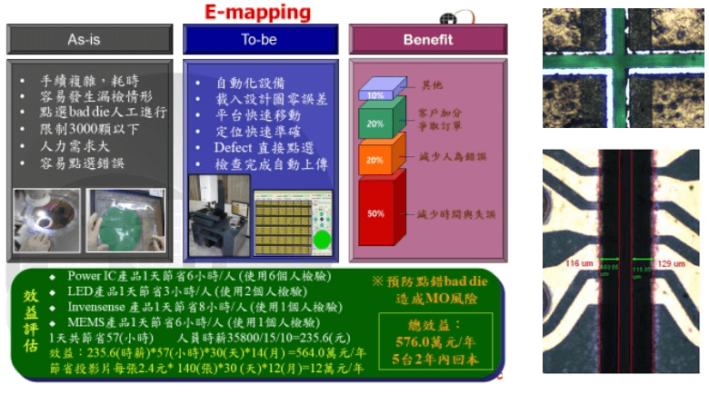
For measuring the height difference distance inside and outside the scribe lane, MiDFUN developed an AOI automatic judgment system. However, because of the optical depth-of-field limitations of high-magnification imaging machines, blurred images were sometimes unavoidable. We believe that after switching to dual-telecentric lenses in 2020, the automation and technology of the microscope machines can break through the current bottleneck. This system retains the option for a coordinated CNC & CIM SECS-GEM upgrade, allowing the current investment and operating methods to be applied to future technologies and machines. MiDFUN continuously adapts to customer needs to develop the most suitable software systems, and we are confident that this will earn customer trust and keep delivering the most suitable products and services.